Course
AI for Semiconductor Manufacturing (ECE 8803 AI4)
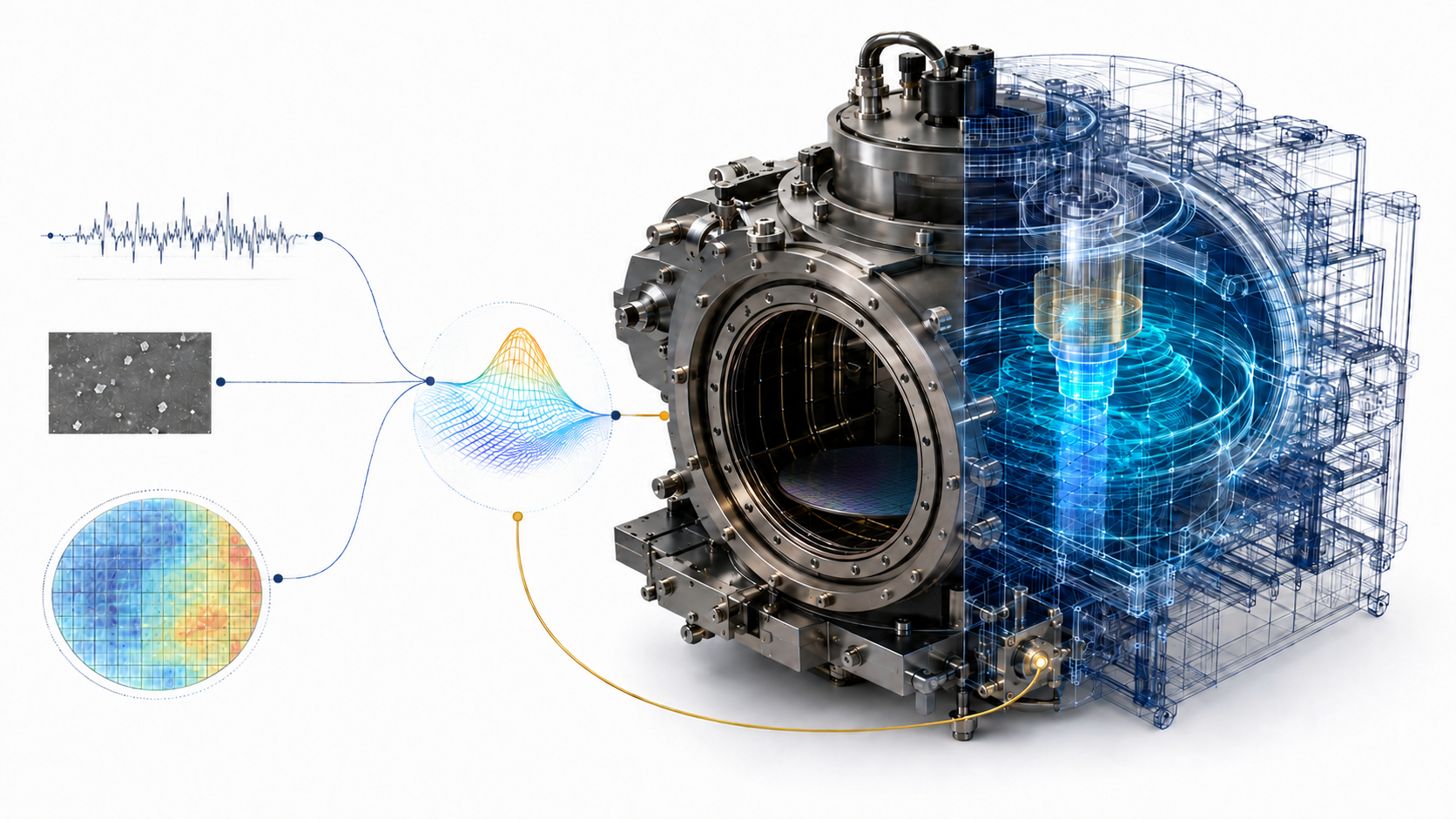
This course explores how artificial intelligence and machine learning can transform semiconductor process technology, metrology, manufacturing, and digital twins through hands-on Python labs, real fab-inspired datasets, and research-driven projects.
The course launched in Fall 2026 as an ongoing graduate course in Georgia Tech ECE, taught by Prof. Asif Khan; this page will continue to be updated as the semester progresses.
The syllabus is available here.
Recorded lectures are available in the YouTube playlist.
Module 1 - Introductions:
Why does semiconductor manufacturing need AI now, and what makes fabs different from ordinary data-science problems? This module frames modern logic, DRAM, and NAND manufacturing as physical, statistical, and economic systems where fab data, metrology, digital twins, process control, and scaling roadmaps determine what AI must actually learn.
Module 2 - Fault Detection and Classification:
How can a fab decide, from sensor traces alone, whether a process run is abnormal before bad wafers move forward? This module treats every process run as a high-dimensional time trace and uses PCA, eigentraces, Hotelling's T2, SPE, anomaly detection, and multivariate SPC to detect excursions, diagnose where they occur, and turn normal-process behavior into actionable control limits.
Module 3 - Defect Classification:
When a wafer map shows failures, what kind of physical defect pattern produced them, and what assumptions does each AI model make? This module compares logistic regression, CNNs, hand-engineered polar features, random forests, and physically interpretable wafer-map features to show that defect classification is a test of what structure the model has learned or assumed.
Module 4 - Agentic AI as a Process Engineer:
Can an AI agent act like a process engineer by proposing, testing, measuring, and revising a semiconductor process recipe? This module uses plasma etch as a closed-loop optimization problem where LLMs, agentic AI, digital twins, simulation, recipe tuning, metrology feedback, and baseline comparisons determine whether the model is engineering or merely guessing.
Module 5 - Statistical Process Control:
How do fabs distinguish real process change from noise, and when is a stable process still not good enough? This module builds the statistical language of manufacturing control through SPC, control charts, run rules, Cp/Cpk, gauge R&R, measurement error, process capability, APC, and AI-based monitoring.
Module 6 - Virtual Metrology:
Can software become a metrology tool, predicting wafer-level measurements fast enough to control the fab? This module turns sensor traces into wafer-level features and uses virtual metrology, PLS regression, cross-validation, high-dimensional modeling, drift monitoring, residual control charts, and run-to-run control to ask when model predictions can safely stand in for measurements.
Module 7 - Test & Qualification:
How can AI help decide whether a chip works today, and whether it will still work years from now, when the data are either massively imbalanced or painfully scarce? This module connects semiconductor test, rare-defect screening, class imbalance, reliability qualification, lifetime extrapolation, uncertainty, physics-based priors, and cost-aware ML to the decisions that determine whether a product can ship.
The following modules are coming as the Fall 2026 semester progresses.
Module 8 - Toolchain, Workflow, and Deployment:
How does a useful notebook become a model a fab can trust and maintain? This module follows the CRISP-DM workflow through Jupyter, Colab, GitHub, PyTorch, MLflow, Gradio, fab data systems, deployment, monitoring, drift detection, retraining, and SHAP-based interpretability.
Module 9 - Transfer Learning and Domain Adaptation:
How can a model trained on one chamber, product, or process node survive when the fab changes around it? This module uses fine-tuning, feature reuse, domain adaptation, hierarchical models, chamber matching, node-to-node transfer, and negative-transfer analysis to ask when prior data help and when they mislead.
Module 10 - Generative Models for Scarce and Imbalanced Data:
Can AI create useful semiconductor data precisely where real examples are rare, expensive, or imbalanced? This module connects autoencoders, VAEs, diffusion models, synthetic defect generation, rare-class augmentation, inverse design, and downstream validation on real held-out data.
Module 11 - Physics-Informed Machine Learning:
How can machine learning respect the physical laws that semiconductor processes must obey? This module explores PINNs, hybrid models, residual learning, governing equations, inverse problems, parameter identification, operator surrogates, and the boundary between data-driven models and traditional solvers.
Module 12 - Bayesian Optimization and Design of Experiments:
When every experiment costs wafer starts, tool time, or simulation hours, where should the next run be placed? This module uses Gaussian processes, acquisition functions, constrained optimization, multi-objective tradeoffs, multi-fidelity learning, and design-of-experiments logic to optimize semiconductor processes efficiently.
Module 13 - Reinforcement Learning for Process and Design:
What changes when semiconductor optimization becomes a sequence of decisions rather than a single best setting? This module introduces Markov decision processes, bandits, policy learning, adaptive test, autonomous experimentation, place-and-route, and sample-complexity limits that shape where RL can actually be deployed.
Module 14 - AI in Design and Electronic Design Automation:
How does AI connect manufacturing constraints back to the design choices that create them? This module covers design-technology co-optimization, compact modeling, computational lithography, tapeout flow, agentic AI in chip design, simulation-driven design, and the link between EDA and fab-aware digital twins.